- Details
- Last Updated: Saturday, 24 December 2022 19:10
Goal: Identification of Atomic Cluster defects in silicon through matching First Principle Calculations and IR Absorption Lines measured using Synchrotron FTIR.
Grown-in defects in ultra-high purity silicon can evolve in a myriad of ways during wafer heat treatments. These defects continue to be problematic for microelectronic industry, as device features continue to shrink. That is why the mechanisms by which point defects are introduced in the crystal, atom complexes form, nucleation occurs, nuclei grow or dissolve... have been subjects for research for several decades. A wealth of experimental data about the distribution and the structure of extended defects (i.e., precipitates, octahedral voids, oxidized voids, dislocations, and stacking faults) has been published.
|
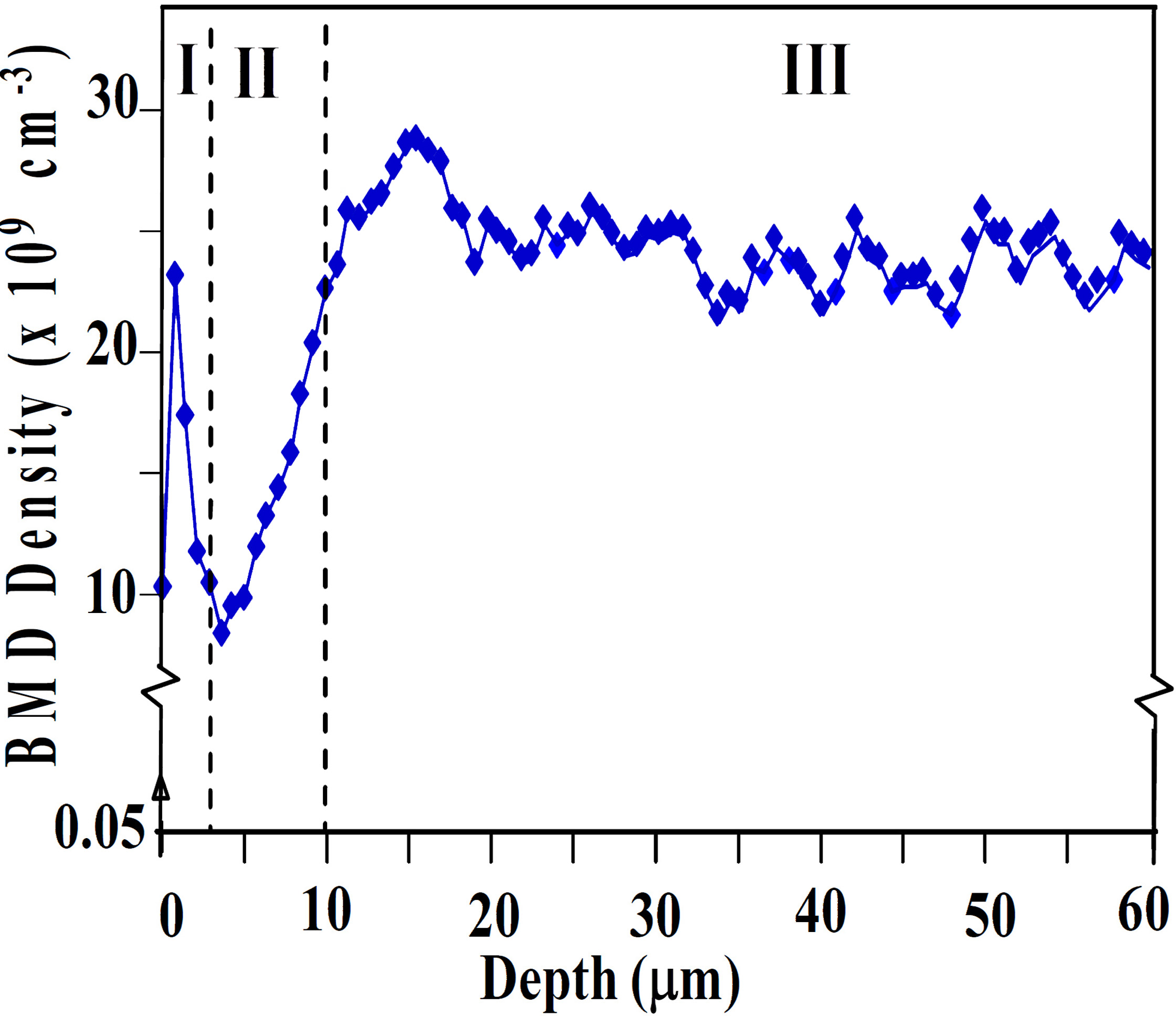
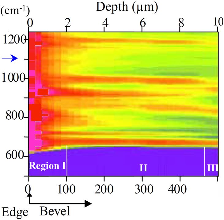
The main goal of this work is the identification of Atomic Cluster Defects in silicon. It combines First Principle Calculations of IR Absorption Lines and measured IR absorption spectra. We focus on chemical complexes [1] detected by FTIR, which were believed to dominate the nucleation and growth of extended defects and to significantly affect the electronic properties of silicon (e.g., thermal donors, recombination centers, traps). We could produce a multitude of atomic species by changing the heat treatments of silicon test wafers annealed with Lo-Hi-Lo and Hi-Lo processes. The composition of oxynitride precipitates was obtained by HR-TEM/Z-contrast and EELS and high resolution SIMS at different depths, starting from the surface. The observed dramatic out-diffusion in NCZ Si wafers, which is more prominent than in the case of crystal growth, permitted to obtain SiOxVyNzIt species at various stages of growth. As example, bands of oxynitride precipitates shown in Fig. 1 spread from the bulk to the surface; their distributions were found extremely intriguing. In particular, the periodic tail of oxynitride precipitates, the “denuded zone”, and the near-surface zone. The latter has a high density of precipitates; of course, this has been the most troubling for microelectronic industry and silicon manufacturers. Defect formation mechanisms in the near-surface zone had to be well understood in order to control them, and possibly prevent the formation of precipitates in the device zone. FTIR spectra data were harnessed with our theoretical models of chemical complex formations, to identify all lines detected in these materials and to build the thermal history of defects. Synchrotron FTIR enabled precise detection of the majority of predicted stable SiOxVyNzIt species in NCZ and NFZ silicon, both in as grown and heat-treated silicon. The major benefit of the Synchrotron FTIR is the sub-micron to micron spatial resolution in addition to the excellent spectral resolution. Fig. 2 shows an IR spectral map of silicon bevel polished heat treated N-CZ sample. |

Fig. 1: Defect depth distribution by OPP in Lo-Hi cycled wafer. Fig. 2: Reflectance spectra by HR-FTIR along bevel polished sample (Bevel magnification factor: 50). 
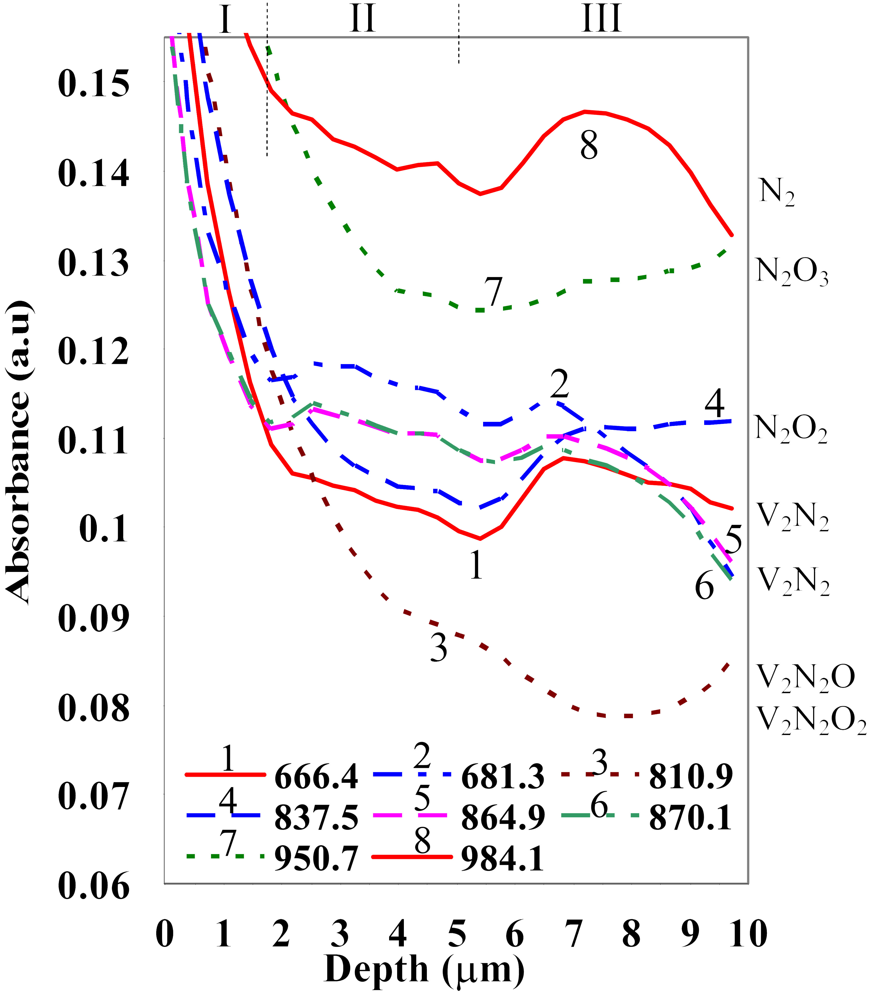
Fig. 3: Intensity of absorption lines (measured from the base) of annealed N-CZ Si wafer. 
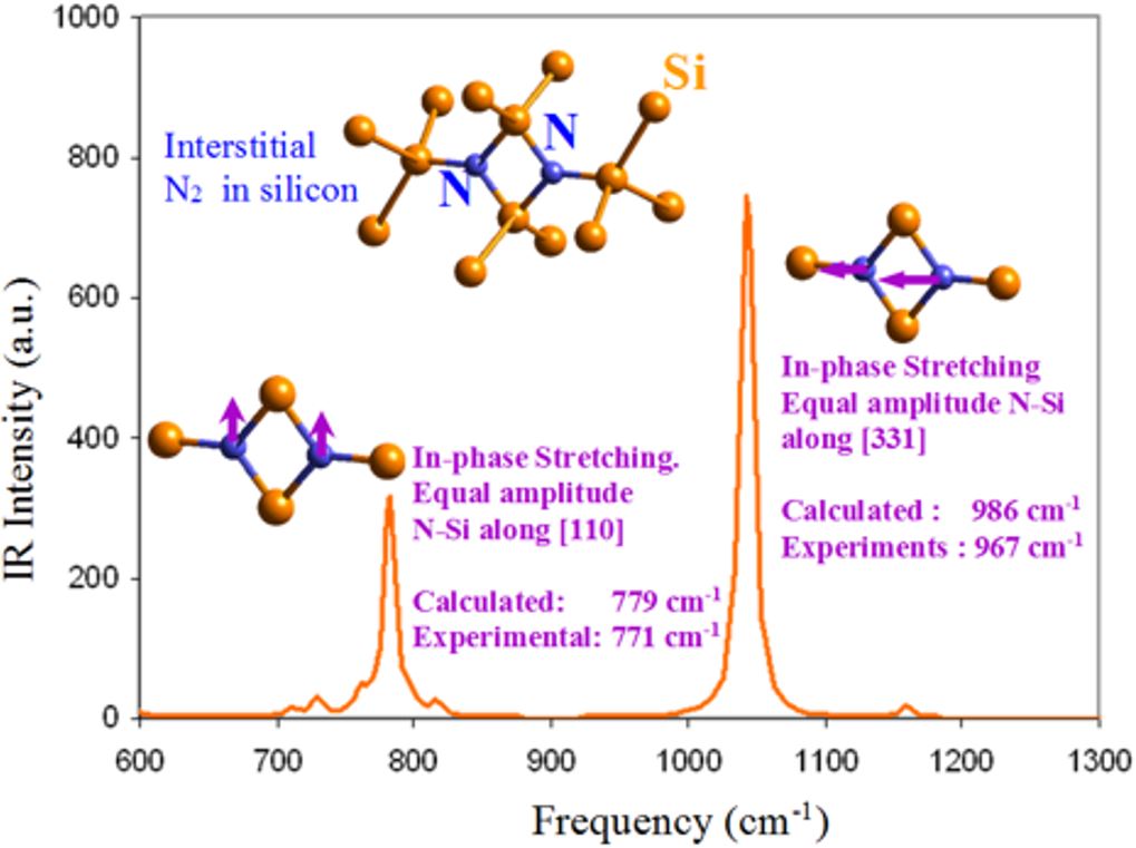
Fig. 4: DFT calculated IR absorption lines of nitrogen defects in silicon. |
|
|
Both as-grown and heat treated silicon appeared to have a rich variety of SiOxVyNzIt complexes. Hence, we took advantage of the high spatial resolution of Synchrotron FTIR and applied it for bevel-polished specimen. This allowed a subtractive approach for filtering out the various species along the depth of beveled samples. Some of the results of the spatial filtering and the FTIR-theory based identification of the O-N complexes is compiled in Fig. 3. As can be seen, the large variety of atomic complexes were detected along the depth and were precisely identified. Other information from HR-TEM/EELS and SIMS showed that they are dissolved in the silicon matrix or constitute the precipitates. The detected oxynitride precipitates appeared, in fact, to have evolved in different ways during their growth, which resulted in variation of the stoichiometries and the atomic structure. The wide variations in the defect growth dynamics was caused by the variation of point defect concentrations with the depth, as well as the local stresses that changed the diffusion dynamics in the near surface zone. Extensive semi-empirical and ab-initio quantum calculations were done to obtain the equilibrium atomic structures of the chemical complexes (by relaxing the species atomic structure of the cluster, i.e., geometry optimization). The investigated complexes were found to have various atomic structures and symmetries, and involve one or more vacancy or interstitial silicon sites. The conformal space, the transition states, and the enthalpy of formation of each of these complexes were calculated. By analyzing the energy data, we could ascertain thermodynamically viable complexes (i.e., most negative Gibbs free energy). Vibrational spectra for stable species were also obtained by both semi-empirical and Density functional theory (DFT) quantum calculations. The symmetry of viable complexes were thoroughly studied for they define whether the vibration is Raman or IR active. DFT calculations have given extremely accurate results for the vibrational spectra. As example, Fig. 4 gives the calculated and measured spectral lines for interstitial N2 in silicon. The theoretical results matched, indeed, very well the experimental FTIR spectroscopy data within 1 and 2%, depending on the spectral line. Our analysis of measured spectral lines in conjunction with first-principle calculations of vibrational spectra appeared to be a powerful way to verify whether predicted specie exists naturally or not. It also allowed measuring accurately the concentration of nitrogen in silicon. |
[1]: Studied oxynitride complexes in silicon are written as: SiOxVyNzIt: where, I: silicon interstitial, V: silicon vacancy, and x, y, z, t = 0, 1, 2, or 3.

