- Details
- Last Updated: Saturday, 24 December 2022 19:13
Goal: Fabricate and Characterize Porous Materials for High Efficiency Solar Cells, Sensors, and Optoelectronics.
We fabricated nano-porous silicon (PS) and nano-porous alumina (PA) for high efficiency solar cells and sensors by combining photolithography and electrochemical etching. Subsequently, we studied structure and optical properties the fabricated porous materials in order to functionalize them for bandgap engineering, the emphasis being on indirect bangap materials.
|
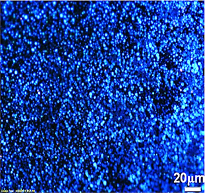
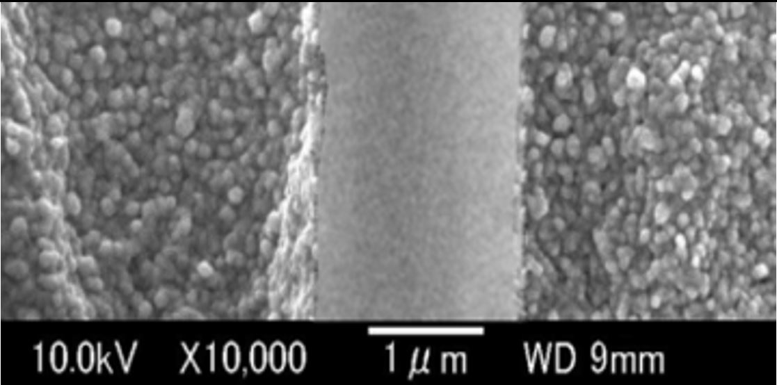
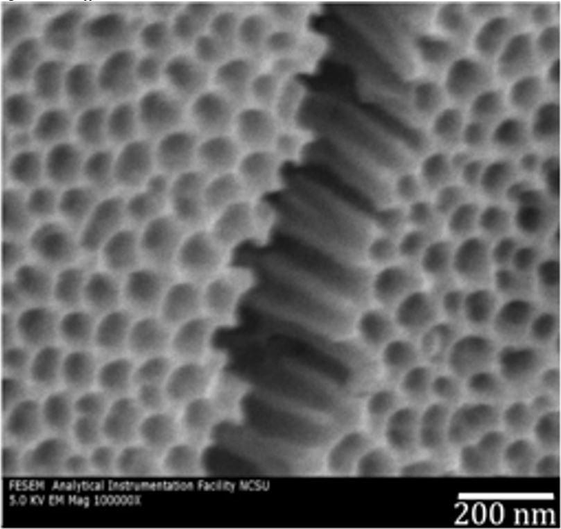
The functionalization of these materials is done through either the growth of nanocrystals on the pore walls, or the adsorption of quantum dots or dies. One of the objectives of the functionalization of interest is to increase light absorption of silicon solar cells. The Nomarski image in Figure 1 shows a macro-porous silicon obtained by a two step electrochemical etching two obtain micrometer sized pores. The material was made on a flat pre-treated p-Si wafer. The porous silicon process is intended for layer transfer and wrap-through solar cell technologies. Figure 2 shows luminescence microscopy image of nanoporous silicon obtained under UV illumination. The specimen was prepared for 3rd generation solar cells, using one step electrochemical etching process. Figure 3 shows a Scanning Electron Microscope (SEM) cross-section image of porous silicon grown by electrochemical etching into 2um wide bores for a new design of third generation solar cell. Note the nanstructured silicon material inside the bores. Figure 4 shows a highly ordered columnar nano-porous alumina that we have fabricated for 3rd generation solar cells. We used a multi-step electrochemical etching of a freestanding thin film of aluminum on a silicon groove. The purpose of using freestanding film is technological as well as to evaluate the effects of stresses at the solid-liquid interface on the material. The fracture shown in the image occurred during the extraction of the specimen from the solution. Interpretation of such phenomenon has been based on osmotic forces between the solution and the nanopores. Verification of this theory has been done by finite element analysis modeling of stresses and strain of the alumina pores. A more complete approach based on Casimir forces is being investigated. Understanding phenomena like these led to improving the fabrication process and to maintain the integrity of porous alumina layers. Through process optimization, we could control the material pore distribution and pore size distribution. We arrived at developing sophisticated processes, including enlargement of the pores via a multi-step etching. |
|
|


