- Details
- Last Updated: Friday, 30 December 2022 15:07
Time Dependent Stress, Strain, and Plasticity during SiGe Stack growth
Goal: Analyze the transient stress and strain during SiGe Stack growth and deduce the steady state plasticity.
We have analyzed mechanical properties of SiGe graded layers at the nanometer scale. Other layers caped with ultra-thin, 15nm thick, silicon films were also analyzed. The materials are either for microelectronics, Nano-opto-electronics, or for Third Generation Solar Cells.
The silicon cap was extremely strained and provided a high carrier mobility material, particularly useful for high-speed electronic devices. The SiGe layers were grown at high temperature by LP-CVD, through 32 process steps, which included temperature ramp-up, deposition and/or annealing, ramp-down, cooling, and some CMP surface polishing. The latter is done on layers that develop defect microstructure at the surface, due to excessive strain.
|
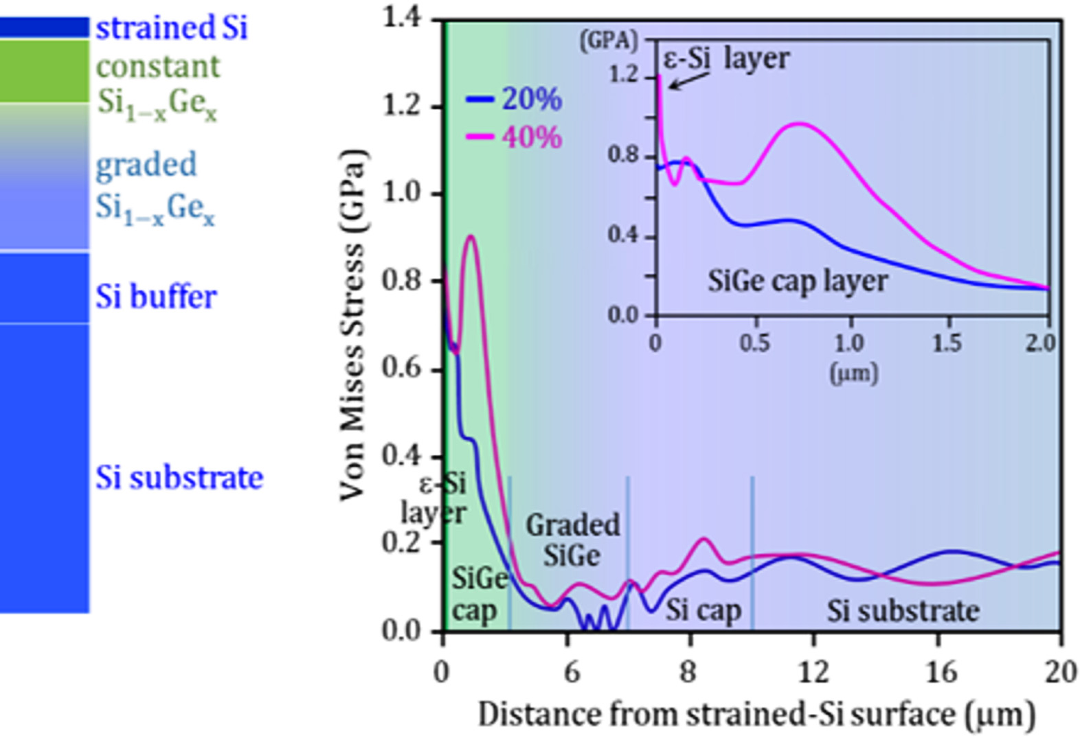
During these steps lattice and thermal expansion mismatches cause elastic and plastic strains. When the SiGe layer reaches critical thickness, the material relaxes by generating a high density of dislocations. The dislocations represent a great issue for microelectronics as well as for solar cells because. They swiftly sink photogenerated currents. To improve the SiGe layer growth process, we calculated the elastic and plastic stresses and strains in each layer. The calculations for the sequence of 32 steps were done by transient FEA in a unique fashion. We could perfectly simulate the growth of the layer stack. The obtained elastic, see Fig. 1 (b), and plastic strains and residual stresses within each layer allowed the calculation of several other essential mechanical proprieties. For instance, we obtained misfit and threading dislocation densities within each layer, in excellent agreement with experimental data. |
(a) (b) Fig. 1: (a) cross section of SiGe stack, (b) Elastic deformation of SiGe/Si heterostructure (strained silicon on SiGe virtual substrate). |

