- Details
- Last Updated: Saturday, 24 December 2022 19:10
Defect Nucleation during Silicon Crystal Growth
Goals: 1) Based on structural, chemical, and spectroscopic data on defects generated from as grown and processed wafers and ingots, develop theories that explain Point Defect Generation, Interaction, Transport, and Clustering in pure silicon, and 2) Experimental validation of the constructed theories.
As microelectronic devices and IC features have been squeezed to a critical level, detailed understanding of defect dynamics during silicon wafer heat treatments have become crucial as to allow control of micro- and nanoscale defects. Practically, the size of defects in the oxygen-rich Czochralski (CZ) silicon is reduced by slightly doping the material with nitrogen. However, industry demanded further control of precipitates and other extended submicro- and micro-defects. To that end, the root cause of defect formation had to be thoroughly studied at various scales. Our work in these areas included the study of defect nucleation and growth in CZ and N doped CZ silicon. It was sponsored by several silicon manufacturers, as well as NREL and the photovoltaic industry. Furthermore, they were interested in similar issues arising in float zone (FZ) silicon and N doped silicon sheets and ribbons for photovoltaic applications.
The objectives of this study include the understanding of:
- Clustering of point defects during silicon crystal solidification,
- Interaction of point defects and light elements (N, C, and O) as silicon crystal, being grown, cools down,
- Extended defect Nucleation,
- Defect growth and annihilation during silicon ingot solidification and wafer heat treatments, and
- Formation of a variety of extended defects and their distribution in OSF rings in Czochralski silicon.
Wafers from specially grown silicon ingots were provided to us via cooperation with the Silicon Wafer Engineering and Defect Science (SiWEDS) consortium member and from NREL. We heat-treated them under various annealing conditions in order to extend our data on defect thermal history. However, no data on early stage defect formation, from the melting point down to 1200°C, could possibly be obtained. Thus, our work relied on multiscale defect modeling with the physics being devised based on thermal history of grown-in defects. The thermal history is constructed by depicting nano- and micro-defects in heat treated silicon wafers. We essentially measured the defect size distribution by OPP, and etching/ Nomarski microscopy (or AFM), analyzed the defect structure by TEM and HR-TEM, the elemental composition of the defects by SIMS as well as EELS/TEM, recombination activity of the defects by micro-PCD, and the electronic properties by PL and DLTS.
The size distribution of precipitates, voids, and stacking faults were calculated for various heat treatments by solving Fokker Planck equations. These were coupled with a set of continuity equations (one for each species involved in the formation of the extended defect) and boundary and initial conditions (one set for each species). Stochastic rate of defect growth and rate of dissolution were considered, along with local stress and strain models, and defect shape considerations.
Physics models for the injection of point defects at the solid-melt interface and the subsequent clustering during crystal cooling and during wafer heat treatments were constructed. The point defects included vacancies (V), interstitials (I), light elements, and impurities. The VO, VN, and NO complexes played a great role in the nucleation of extended defects during silicon crystal growth.
Fig. 1: Basic mechanism of extended defect formation in CZ-Si based on the model of “V-O clustering pathways” by Bae, Rozgonyi, and Karoui.
Fig. 2: Karoui's model for point defect clustering mechanisms in the N-Cz.
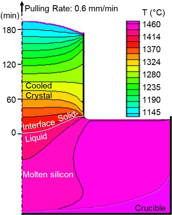
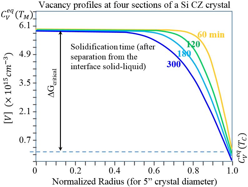
Fig. 3 (a) provides simulated temperature profile in a Si crystal being pulled, the profile is extended in the volume of the crucible. This crucial information was used to calculate the diffusion of point defects and clusters for various initial profiles at the melting-solid interface. Fig. 3 (b) shows the vacancy profile at different levels of the ingot; the V concentration is significantly reduced at the crystal rim as the ingot is cooled down.

(a) (b)
Fig. 3: Finite Difference Time Domain modeling of silicon CZ growth: (a) Temperature distribution during crystal pulling (b) Profiles of vacancy atomic defects in four sections of the silicon crystal ingot.
The outcomes of this research were extremely useful for improving the quality of ultra-high purity Si crystals and Si wafer heat treatments. They have been used by microelectronics industry members of the SiWEDS consortium sponsored by NSF (Sumitumo Sitix, Nippon Steel Corp. and Wacker). Our partner Dr. Deren Yang (Silicon Key Lab., China) has contributed in the growth of N doped Cz silicon.
This multi-facet study was complemented by experimental work on clustering of point defects in N and C rich Si for photovoltaics and gettering of light elements by grain boundaries and dislocations. Notably, NREL (Dr Ted Cizek) has grown for my research special N doped FZ silicon ingots for photovoltaics. Work on thin polycrystalline silicon wafer was sponsored for my group by BP Solar. Likewise, N- and C-rich multicrystalline silicon sheets and EFG silicon sheets were provided by Astropower and Evergreen, respectively.

