- Details
- Last Updated: Friday, 30 December 2022 15:06
Mechanical Properties of Polycrystalline Silicon wafers
Goal: Analyze the mechanical properties of Ultra-Thin Polycrystalline Silicon to control Wafer Breakage and to increase Solar Cell Fabrication Yield.
There has been a continuous appeal for reducing the thickness of crystalline silicon wafers in order to cut the cost of solar cells. However, this necessity is hindered by an increased wafer breakage during solar cell fabrication on ultra-thin wafers, especially for polycrystalline silicon, a material of great hope for photovoltaics.
In addition, to the handling of the ultra-thin wafers, excessive local stress build-up (during and after high temperature processing) increases the causes of solar cell breakage. As a result, the yield of solar cell fabrication on ultra-thin polycrystalline silicon is significantly lowered, which has become problematic for the photovoltaic industry. At one point, the yield problem, if not solved, appeared to compromise the future of silicon based photovoltaic technology. We proposed to BP Solar and NREL to study this crucial problem based on a newly devised approach, in which local mechanical properties are assessed and correlated to local material composition and defects. The study focused on the effects of structural and chemical defects on wafer toughness reduction. It allowed the analysis of i) cast polycrystalline Si thin wafers from BP Solar (home-grown material used in their solar cell production), and ii) FZ wafers grown at NREL. We could discern the factors that cause fractures to occur during and after heat treatments, which offered means to predict the likelihood for wafer breakage. Both grain morphology and lifetime information are measured in a non-invasive way, and used to determine the critical defects that cause wafer breakage. This was the salient feature of our research method. The non-invasive metrology method was intentional used for it is useful in production.

(a) (b)
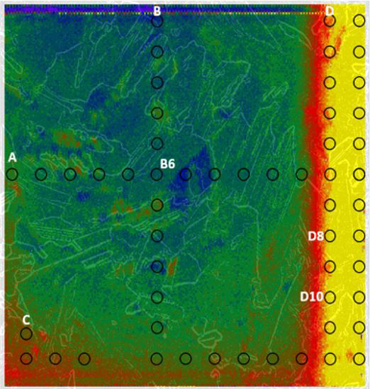
Fig. 1: a) Superimposed lifetime and GB maps of 5” Si wafer; the circles show special locations of samples used in disc bending test, b) Bending test results for three samples.
Recombination lifetime, see Fig. 1(a), was mapped with Amecon Janus 300, which has a spatial resolution of . I could correlate grain size and grain shape parameters (calculated from the image of etched wafer) with the measured local recombination lifetime. The effective yield stress was delineated by disc bending tests, see Fig. 1(b) and by nano-indentation. The fracture mechanisms were correlated to lifetime. Impurities responsible on the lifetime variations were determined by DLTS along with their concentrations.
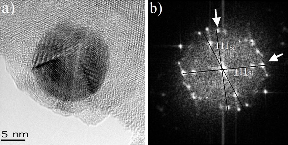
Fig. 2: a) HR TEM micrograph of metal precipitate found in the near surface of silicon wafer; b) The arrows in the FFT image indicate principal reflection plans of the precipitate. Unusual epitaxial relationship is observed and at the interface silicon-precipitate, indicative of a non-equilibrium defect in the silicon matrix.
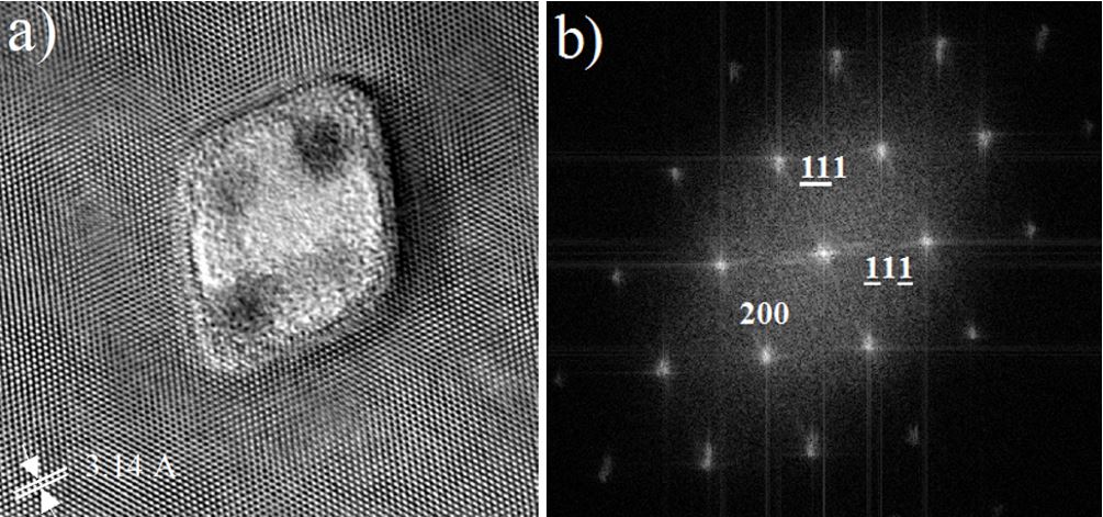
Fracture events were found to nucleate on crystallite metal precipitates, such as the one shown in Fig. 2, and rarely on amorphous precipitates like oxynitride precipitates, see Fig. 3. The former was detected in silicon contaminated with copper, while the latter was detected in N doped CZ silicon. Crystalline precipitates generate more strain in silicon matrix, compared to equilibrium amorphous oxynitride precipitates. The latter stop punched-out dislocations once they start to move. As a result, fracture events are delayed and wafer toughness is increased.
Fig.3 a) HR TEM picture of the amorphous precipitate b) FFT of the same precipitate. Facets are parallel to planes.


