- Details
- Last Updated: Saturday, 24 December 2022 19:13
Detection of Extremely Low Impurity Concentration in Ultra High Purity Silicon
Goals: 1) Detection and analysis of Impurities in silicon with Extremely Low Contamination, and modeling charge carrier recombination and trapping, 2) Use ultra-clean Rapid Thermal Processing as experimental model, and 3) Enable defect-free RTP process development by controlling both structural and impurity defects (i.e., push down the contamination to below the detection limit offered by the most advanced techniques).
|
As rapid thermal processing (RTP) has become important for microelectronics, Mattson Technology (Fremont, CA) a microelectronics tool manufacturer and member of the SiWEDS has contracted me to 1) diagnose process induced micro-defects in large silicon wafers processed by their Aspen RTP system, 2) develop means to control these defects, and 3) analyze and solve the issue of contamination that occurs during wafer processing and which was below the known detection limits. The salient features of the Aspen RTP tool is the ability to attain extreme temperatures, fast ramp-up and ramp-down, and fast thermal cycling. The ultimate goal of our defect analysis was to improve Mattson's state of the art RTP tool for microelectronics. The tool was originally designed for 90nm node, and evolved to 32nm thanks to our research findings. This undertaking included detection of extremely low concentration of impurities, which were at the frontier of detection limits of the most sensitive techniques (uPCD and DLTS), structural analysis of RTP process-induced defects, and understanding the mechanisms of defect generation by ultra-fast thermal processes and the subsequent defect growth in such severe environment. The scientific challenges hinge on the involved transient thermal phenomena, the Si mechanical wafer response to the extreme thermal and stress conditions, and the extremely low concentration of chemical impurities, which can not be tolerated by microelectronics standards (then node 90nm and projected future nodes). Hence we had to use the most sensitive analytical methods and enhance their capability of detection: uPCD wafer mapping was combined with Limited Projection XRT and with DLTS, Thermally stimulated uPCD, TOF-SIMS... Most importantly, we improved the techniques (for instance, lifetime detection limit was improved by perfecting the wafer surface passivation during uPCD measurement) and we correlated the data to further push the detection limits. |
|
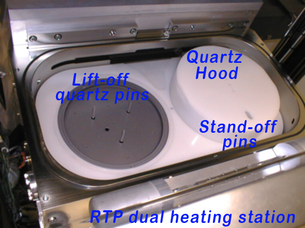
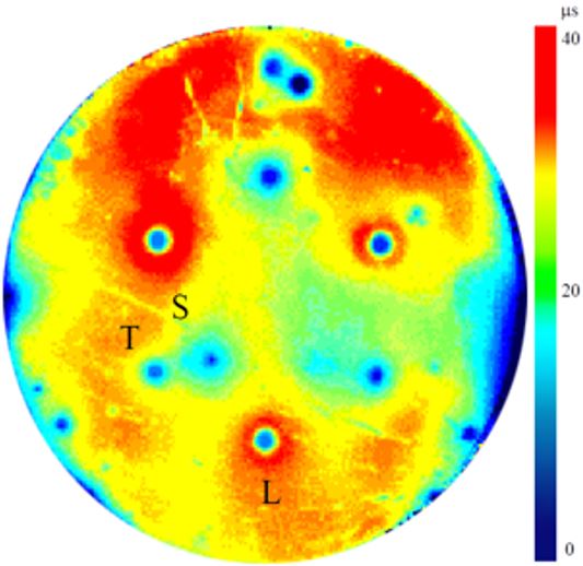
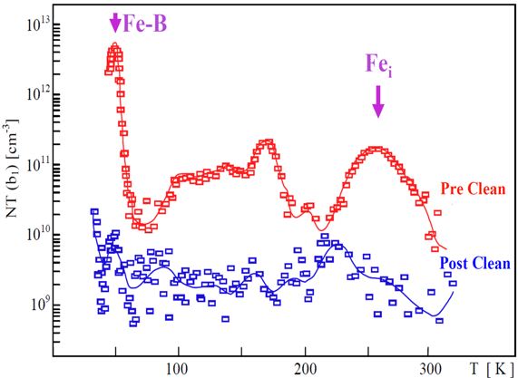
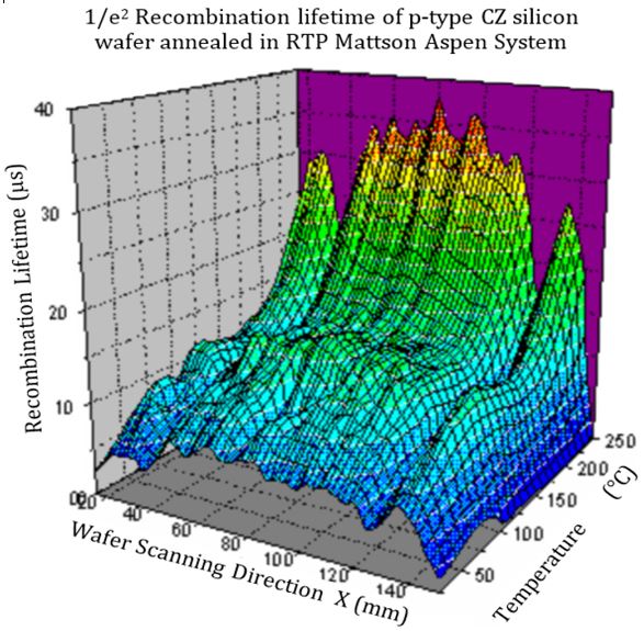
Fig. 1: Processing chamber of the Lamp-Free Aspen RTP system for microelectronics. Fig. 2 shows minority charge carrier recombination map of a 200 mm diam. p-type CZ silicon wafer which was annealed in a lamp-free RTP tool for microelctronics, capable of processing 300mm diam. wafers. The system is totally robotized and handle the wafers on the susceptor with ultra clean quartz hardware. The map was obtained with a high resolution microwave Photo-Conductance Decay (uPCD) in low injection mode. It shows the distribution of electrically active impurities and variations of their activities. The , detected extremely low levels of impurities in RTP wafers, some of these impurities were identified with the help of Deep Level Transient Spectroscopy (DLTS), see Fig. 2, and others with Vapor Phase Decomposition-Inductively Coupled Plasma Mass Spectrometry (VPD ICP‑MS). In p-type silicon, iron either forms interstitial traps (i.e., FeI), or FeB traps by pairing with the dopant. Transition metals are lifetime-killers, as such, they severely degrade carrier lifetime, thus must be avoided during high temperature processing. To that end, a high temperature process that uses on a mixture of reactive gases was developed to decontaminate the RTP Aspen tool. It significantly reduced iron contamination by 2 and 3 orders of magnitude for [FeI] and [FeB], respectively. Both concentrations were reduced to less than 1010cm‑3, which was below active defect threshold defined by the International Technology Roadmap for Semiconductors (ITRS). This result won Mattson the 300mm SEMATECH Award and promoted their $1.2 million worth advanced RTP tool. RTP silicon wafers were also investigated by uPCD as a function of wafer temperature. This technique is spectroscopic in nature; I used it to identify active impurities in silicon. Fig. 3 shows lifetime line-scan versus wafer temperature, varied between 40°C and 250°C. The lifetime variation along the scanned line was attributed to iron concentration variation, based on DLTS measurements. |
Fig. 2: uPCD recombination lifetime showing active impurity distribution in RTP silicon wafer (200 mm diam.).
Fig. 3: DLTS spectra of 2 wafers, one processed before decontamination (Pre Clean) of the RTP system and the second after (Post Clean).
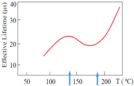
Fig. 4: uPCD lifetime temperature scan across the diameter of 6" CZ Si wafer cycled one time by RTP. Fig. 5: Average minority lifetime variation (over the line-scan) as a function of temperature. The S shape is due to FeB dissociation.
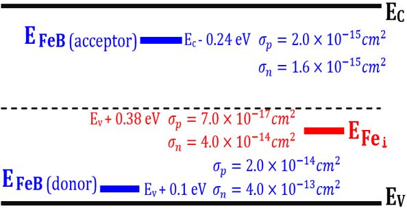
Fig. 6: DLTS determined trap levels in RTP p-silicon. |
|
|
The chart also shows along the temperature axis, the signature of FeB decomposition according to the reaction: FeB --> FeI + B Fig. 5 shows the average lifetime variation with the temperature. An increase up to 130°C is seen; it is attributed to FeB pair decomposition. This process cancels minority carrier (here electrons) recombination, the reason for increased minority lifetime. As shown in Fig. 6, FeB donor level is an effective trap for electrons, more than the other traps since it has higher capture-cross section. Thus, dissociation of this trap allows electrons to survive longer, which explains the lifetime increase. At 130°C, the highly effective FeB traps are dissociated. Beyond that temperature, lifetime decreases as recombination is more favorable with the increase of temperature, the active trap has electron capture-cross section sigman of 4E-14 cm2. Above 170°C acceptor FeB traps further dissociate. If all FeB dissociate, interstitial iron concentration becomes the sum of both species concentrations: [FeI]Final = [FeI]Initial + [FeB] FeI and FeB energy levels and their concentrations in RTP p‑type silicon test samples were determined by DLTS. The data was used to support the trap-assisted recombination model of Shockley-Read-Hall (SRH), which helped analyzing and quantifying carrier trapping and recombination processes in RTP processed wafers. |
||

