- Details
- Last Updated: Tuesday, 27 December 2022 18:26
Ordered Quantum Dot Arrays
Goal: Study the physics of Ordered Quantum Dot Arrays for Quantum Information and Nanosensors.
Research on ordered quantum dot (QD) arrays is moving to revolutionize future engineering fields, including optoelectronics, third generation solar cells and beyond, bioengineering, and nanomedicine, to name a few. We have a strong interest in theoretically deriving the properties of QD arrays, the electron and photon confinement in such quantum systems, and charge carrier transport intra- and out of- QD arrays. Understanding the mechanisms of photons and charge carriers in these systems is essential for developing high performance optoelectronic and quantum computing nanodevices.
|
We fabricate low cost SiGe QD layers using Ultra High Vacuum Rapid Thermal Chemical Vapor Deposition (UHV-RTCVD) and Pulsed Laser Deposition (PLD). Other routes for making QD layers are reported in the literature, but we focus on RTCVD and PLD techniques because they allow production of low cost QD layers over entire wafers. We have succefully grown Ge and SiGe QD layers on 200mm dia. silicon wafers with excellent uniformity using RTCVD. In addition, these techniques can be adopted by industry as they are suitable for production. Such features and others meet our research goals, while allowing us developing excellent photovoltaic and optoelectronic devices, as well as contributing in the integration effort of QD layers with microelectronic technologies. Electron localization and tunneling in laterally distributed QD ordered arrays have been studied. A quantum well is induced by each QD. The QDs and associated electrons behave like aritificial atoms and the array behaves like a molecule. The fact that the physical and chemical properties of the QD can be easily modified allows changing the physical properties of the quantum system, unlike real atoms and molecules. This provides great technological relevance. We have studied the effects of QD shape variation and asymmetries on the propereties of electrons bond ot the QD. Adding a quantum well has been investigated as a weakly coupled component to the array. To that end, InAs/GaAs QWs were modeled using single sub-band effective mass approach with effective potential simulating the strain effect. When the QDs are coupled, their energy specta are altered, and various states (doublet, triplets, quadruplets,...) are manifested. In some instances electron confinement can induce doublet-triplet or - quadruplet transitions. Electron localization dynamics in small quantum dot arrays (known as double and triple quantum dots: DQD and TQD) over the whole spectrum is studied in relation to the inter-dot distances and strymmetry breaking (by slightly varying the dot shape and size). The electron tunneling appeared highly sensitive to small symmetry violations. We showed that the introduction of a new dot increases the tunneling in the intial QD array. The dependence of the tunneling in QD arrays on inter-dot distances and symmetry breaking has been investigated according to tuneling and chaotic behavior of electrons. Our approach to making nanosensors is based on the use of ordered QD arrays (i.e., almost identical quantum dots within symmetric arrays). Various lattice types have been |
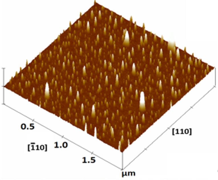
AFM image of SiGe quantum dot layer grown by UHV-RTCVD.
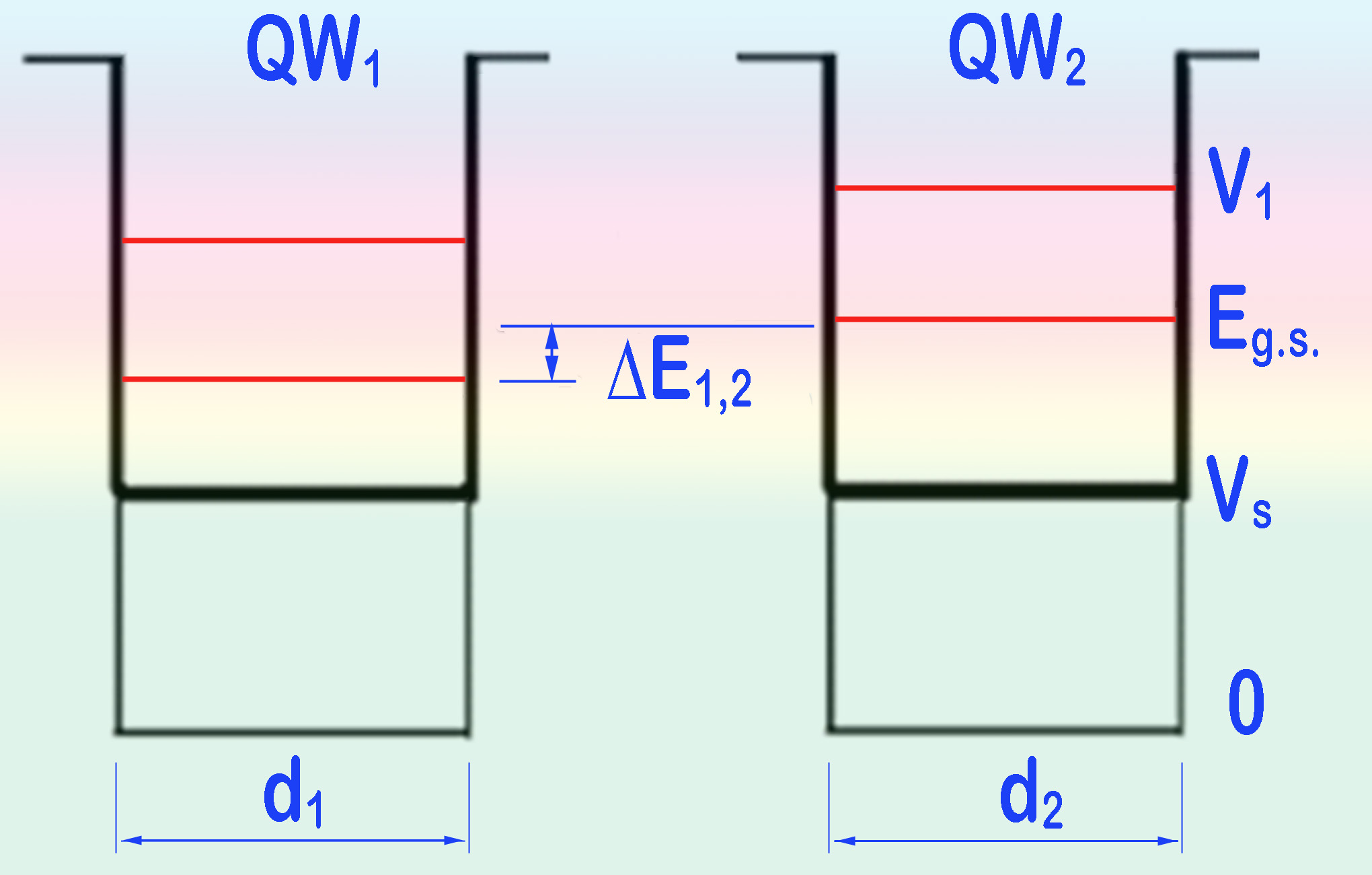
Electron energy band structure of two isolated QDs. A Quantum Well (QW) is associated to each QD along with the intrinsic energy spectrum. The two spectra differ as the two QDs are not identical. 
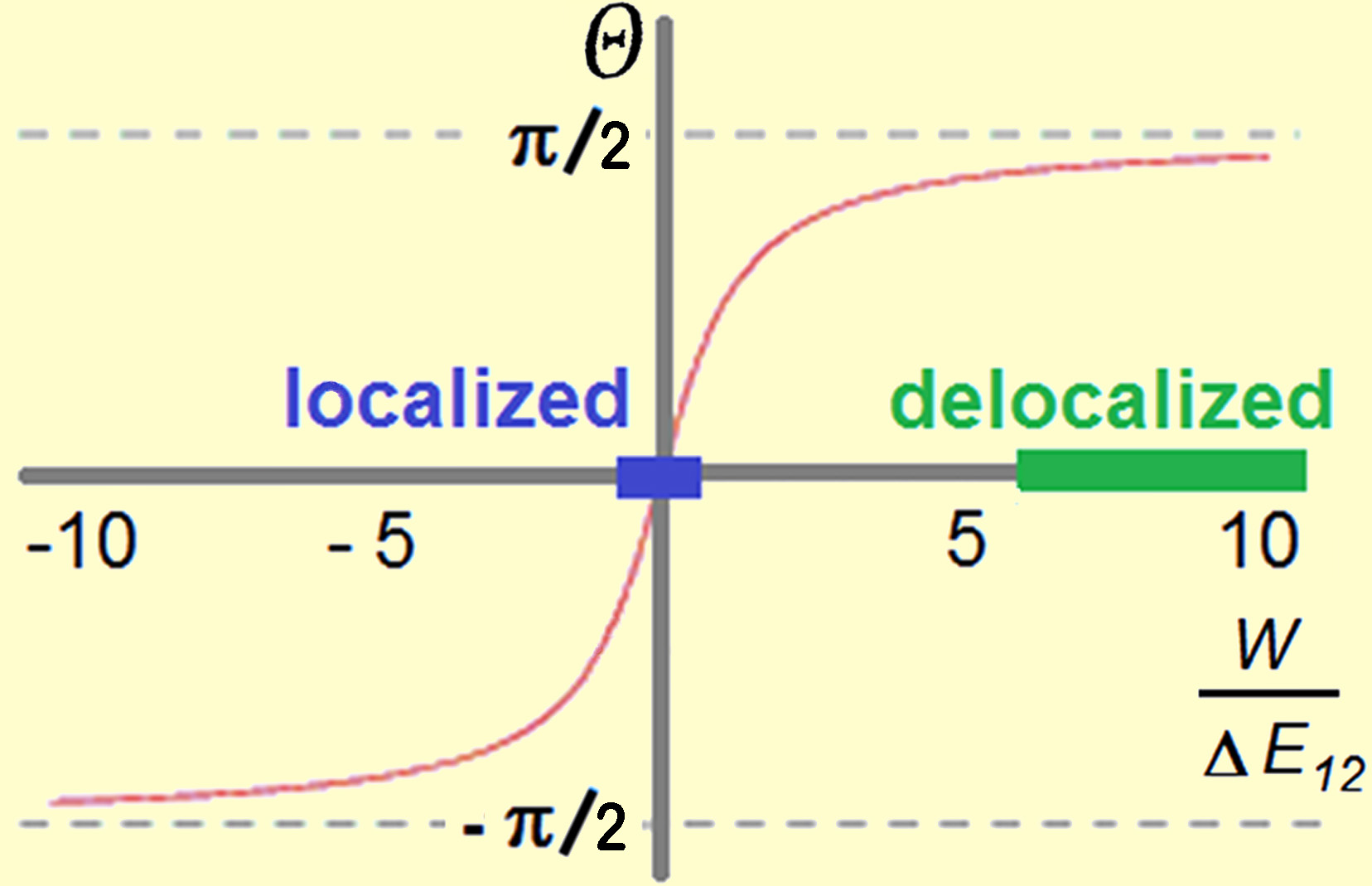
Electron Localization and Delocalization as a function of the energy level difference in weakly coupled QDs.
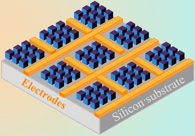
Principle of ordered QD array based nanosensor. |
|
|
considered: QDs organized in square lattice as well as QD rings. The study includes electron confinement, electron transport through tunneling within the quantum dot array and to/from external leads. Ordered quantum dot arrays are selected from large areas, isolated, and employed as the core functional part of the nanosensor. |
||
STILL UNDER CONSTRUCTION
(please come back later)


