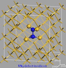
Goal: Identification of Atomic Cluster defects in silicon through matching First Principle Calculations and IR Absorption Lines measured using Synchrotron FTIR.
Grown-in defects in ultra-high purity silicon can evolve in a myriad of ways during wafer heat treatments. These defects continue to be problematic for microelectronic industry, as device features continue to shrink. That is why the mechanisms by which point defects are introduced in the crystal, atom complexes form, nucleation occurs, nuclei grow or dissolve... have been subjects for research for several decades. A wealth of experimental data about the distribution and the structure of extended defects (i.e., precipitates, octahedral voids, oxidized voids, dislocations, and stacking faults) has been published.
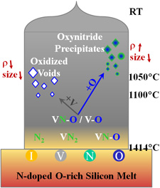
Defect Nucleation during Silicon Crystal Growth
Goals: 1) Based on structural, chemical, and spectroscopic data on defects generated from as grown and processed wafers and ingots, develop theories that explain Point Defect Generation, Interaction, Transport, and Clustering in pure silicon, and 2) Experimental validation of the constructed theories.
As microelectronic devices and IC features have been squeezed to a critical level, detailed understanding of defect dynamics during silicon wafer heat treatments have become crucial as to allow control of micro- and nanoscale defects. Practically, the size of defects in the oxygen-rich Czochralski (CZ) silicon is reduced by slightly doping the material with nitrogen. However, industry demanded further control of precipitates and other extended submicro- and micro-defects. To that end, the root cause of defect formation had to be thoroughly studied at various scales. Our work in these areas included the study of defect nucleation and growth in CZ and N doped CZ silicon. It was sponsored by several silicon manufacturers, as well as NREL and the photovoltaic industry. Furthermore, they were interested in similar issues arising in float zone (FZ) silicon and N doped silicon sheets and ribbons for photovoltaic applications.
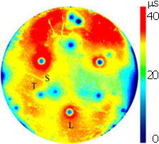
Detection of Extremely Low Impurity Concentration in Ultra High Purity Silicon
Goals: 1) Detection and analysis of Impurities in silicon with Extremely Low Contamination, and modeling charge carrier recombination and trapping, 2) Use ultra-clean Rapid Thermal Processing as experimental model, and 3) Enable defect-free RTP process development by controlling both structural and impurity defects (i.e., push down the contamination to below the detection limit offered by the most advanced techniques).
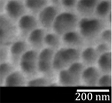
Goal: Fabricate and Characterize Porous Materials for High Efficiency Solar Cells, Sensors, and Optoelectronics.
We fabricated nano-porous silicon (PS) and nano-porous alumina (PA) for high efficiency solar cells and sensors by combining photolithography and electrochemical etching. Subsequently, we studied structure and optical properties the fabricated porous materials in order to functionalize them for bandgap engineering, the emphasis being on indirect bangap materials.
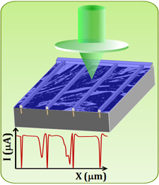
Characterization and Modeling of Defects in Polycrystalline Silicon
Goal: Characterization and modeling of Polycrystalline Silicon Defects using a Modified Light Beam Induced Current (LBIC) to help optimizing Solar Cell Screen Printing fabrication process.
Solar grade cast polycrystalline silicon wafers and multi-crystalline silicon layers have high density of extended defects that are notorious for a strong reduction of solar cell efficiency. Recombination centers and traps (defects decorated with impurities, dangling bonds,...) sink the photogenerated current and shunt the cell junction. Laser/Electron Beam Induced Current (LBIC / EBIC) are excellent techniques for detecting these centers and fully characterizing their recombination activity. They were originally designed to analyze grain boundaries (GBs), precipitates, and dislocations.
More Articles ...
- 1.b.10. Gettering of Oxygen and Carbon in N-rich Multicrystalline Solar grade Silicon
- 1.b.11. Mechanisms of Oxygen Precipitation in N-CZ Si
- 1.b.12. Mechanical Properties of Polycrystalline Silicon to Control Wafer Breakage
- 1.b.13. Time Dependent Stress, Strain, and Plasticity during SiGe Stack growth
- 1.b.14 MEMS for Handling and Processing Nanotubes and Nanorods
